What is a PCBA ?
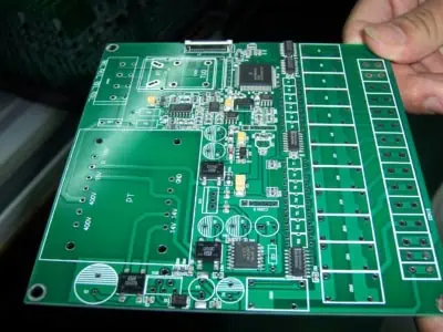
PCBA stands for Print Circuit Board Assembly, it consist of an electronic board (PCB) assembled with electronic components. It can be used to control electrical power supply, lightings, computers, or even a vehicule. How PCBA manufacturing is organised ? Read the below article to learn more about it.
PCBA manufacturing process
Electronic circuits assembly is a sensible and relatively complex process. It follow different stage, defined below :
1- Raw PCB
The raw print circuit (PCB) is manufactured from a substrate, otfen FR4 polymer which will be covered of copper layers for the conductivity, soldering mask for the welding and finaly marked with silkscreen.
PCB can be monolayer or multilayer, multilayer boards enable more complex connexions between components and therefore a higher density of components.
Silkscreen marking, often white or black, simplifies the positionning of the components but also helps boards identification.
Raw PCB manufacturing process is mainly substrate and masks cutting, plus chemical deposition and bonding of the different layers. As the process is relatively polluting and agressive for the operators, PCB manufacturors are mainly positionned in developing countries (China, south-east Asia).
2-Components assembly
The most critical operation is assembling the components on printed boards. There are for this matter two main process: often referred as Thru-hole and SMT (Surface Mount Technology).
2-1 Component placement
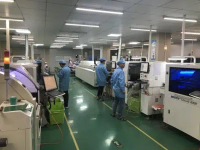
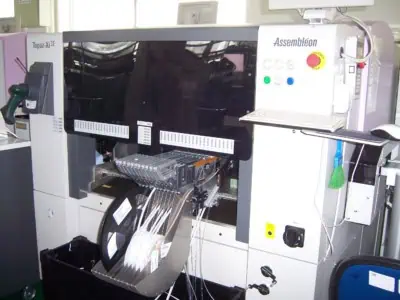
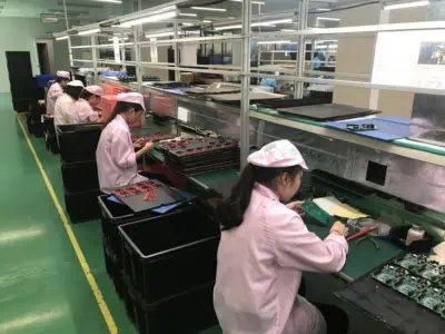
In PCBA manufacturing placement of the components can be made manually (mostly for the Thru-hole components) or with automatic mount machine which are much quicker and works well with very small components (SMD).
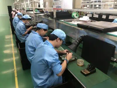
Good placement of electronic components is key to the proper functioning of the PCBA. Many components are not symetric in their usage, meaning they need to be positionned in the good direction. Moreover, quality of the component soldering, which guarantees both good connexion and assembly strength is also determined by component good positionning.
2-2 soldering
Soldering is assured by an alliage of silver, tin and copper; lead is strictly forbidden if RoHS norm is to be respected.
Component soldering is done in oven which heat the soldering mask up to 250°C, at which temperature it starts to melt and bond the components to the board. Assembly is afterwards coolled along a conveyor belt equiped with heat exchanger.
An other semi-automatic process is the use of a soldering wave oven, where the soldering agent is already liquid and will be put in contact with the bottom of the PCB and bonding components legs to it. However, this process only allows components to be soldered on one side.
3-PCBA programming
It is necessary to program different components (microcontrollers, chips) after assembly to enable the functionality of the PCBA. This programming is carried out on designated components by computers via connectors present on the PCBA.
4-Boards protection
Electronic cards being sensitive assemblies, once the assembly of the components has been carried out, it is common to protect them from possible external aggression:
4-1 Conformal coating
The conformal coating is the application of a protective layer on the electronic cards after assembly, this application can be carried out by spraying, dipping or brushing.
Different types of protective layers can be applied: polymer, varnish or silicone for example. These protective layers, a few micrometers thick, protect the cards against humidity, dust, chemicals and improve resistance to high temperatures.
Due to the many treatment references available, an analysis of the advantages and disadvantages of each must be carried out to identify the best protection.
4-2 Potting (resin pouring)
Another protection, heavier to put in place is the potting of the boards, which is usually carried out in an electronic casing, poured with resin in order to completely protect the PCBA from the external elements.
This solution offers better protection than conformal coating, however it has the disadvantage of being thicker, of not allowing access to the cards for possible repair, of requiring a special box, of being bulkier and longer to implement.
5 – Quality control
Due to the complexity of the cards, many factors can cause them to malfunction. It is essential to check the cards during and after manufacture. There are several types of quality controls that can be made to ensure the good results of the PCBA manufacturing process:
- ICT control or “nailboard” which allows by a specific board mounted with many contacts (“nails”) to check different contact points of cards and components.
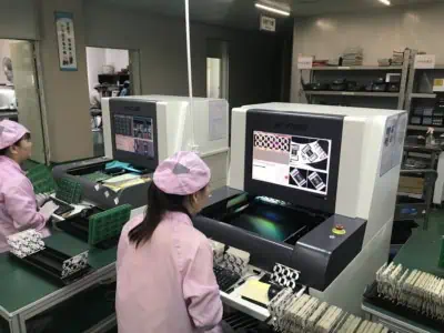
- Vision machine control, these controls allow very fast control rates, the component locations being pre-programmed in the machine. It also enables automatic sorting of the OK and NOK PCBA.
- Visual inspection: carried out by a quality operator, it makes it possible to detect any visible defect of the PCBA.
- UV control, it makes it possible to control the application of the conformal coating which carries fluorescent markers.
- Function test : a test bench is created to test the functionalities of the board and make it possible to sort out faulty boards.
6-Assembly
The last stage of manufacturing will be the assembly of the card with mechanical (connectors, boxes) and electrical (electric cables) components in order to finalize the production of the electronic module. This last step can be carried out by an EMS (electronic card assembler) or another subcontractor.
Special precautions on electronic card assembly lines
In order to minimize the risk of quality problems in production, you will find below the list of some common rules used by the best EMS:
- Individual protection against Electricity Static Discharges ( ESD earthed bracelets worn by operators).
- Assembly done in clean rooms to avoid dust that could create bad contacts on the boards.
- Inspection of components before assembly. (IC Incoming Control)
- Respect for lead-free throughout the production line, if the assembly lines are not dedicated to lead-free there is a high risk of contamination.
- Production monitoring (kanban), in order to avoid operation errors.
- Waste management, electronic components can contain expensive (rare metals) or dangerous materials for the environment, it is important not to mix them with other wastes.
